Semiconductors are materials exhibiting unique electronic properties, their electrical conductivity falls between that of conductors and insulators. Semiconductor materials are used to manufacture components like transistors and diodes, which are integral to electronic equipment.
Semiconductors are used for simpler devices like solar cells and LEDs, but more commonly, they are fabricated into chips that power ICs, microprocessors, memory chips, and communication modules such as Bluetooth, Wi-Fi, and mobile communication. They also play a crucial role in systems like anti-lock braking systems (ABS).
An integrated circuit (IC), also known as a microchip, or simply chip, is an electronic components that integrate millions of transistors and other elements(such as resistors and capacitors), onto a small semiconductor substrate, typically made of silicon.This substrate is known as a chip, which is why ICs are often referred to as chips. These integrated elements collaborate to perform various functions, such as data processing, data storage, signal amplification, or functioning as an oscillator, counter, or logic gate.
[2][3]
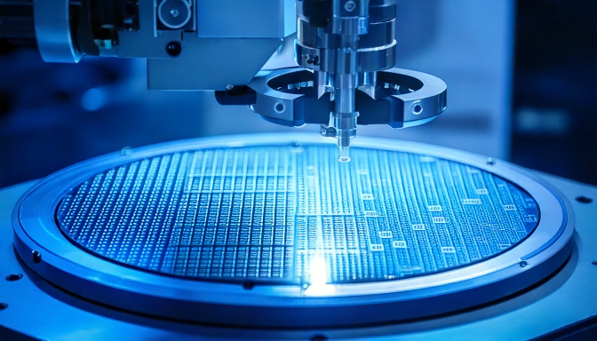
A wafer in electronics is a thin, circular slice of semiconductor material, typically silicon, that serves as the foundation for producing microchips. During the manufacturing process, multiple layers of materials are deposited onto the wafer, and intricate patterns are etched into it to form integrated circuits. This wafer is then sliced into numerous individual components known as chips.
[4][5]
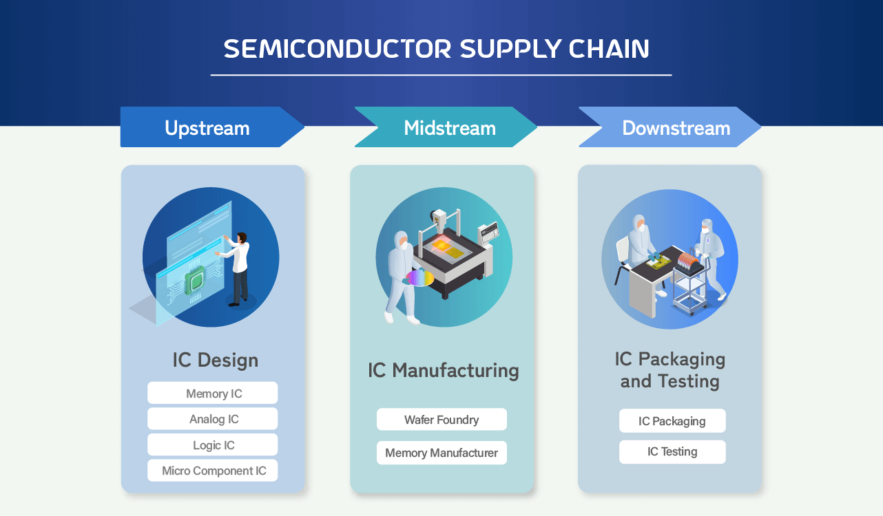
Semiconductor Industry Chain could be simply divided into three segments: IC design, IC manufacturing, and IC packaging and testing.
Many IC design companies are fabless, meaning they design and sell chips but outsource the manufacturing and testing processes. Notable fabless companies include Qualcomm, NVIDIA, Broadcom, and Taiwan semiconductor companies like MediaTek, Novatek, and Realtek.
IC manufacturing is handled by foundries like TSMC and UMC from Taiwan, and GlobalFoundries. IC packaging and testing are performed by OSATs (Outsourced Semiconductor Assembly and Test) such as Taiwan-based ASE and SPIL, along with Amkor and JCET.
There are also Integrated Device Manufacturers (IDMs) like Intel, Samsung Electronics, and Texas Instruments. These companies design, manufacture, package, and test their own chips, managing all segments of the semiconductor industry chain with full production capabilities.
1 ) Upstream Semiconductor Industry
The upstream segment of the semiconductor industry focuses on IC design, where companies create and verify chip functions, turning concepts into chip designs.
- Memory ICs: Store data and program instructions; found in PCs, smartphones, gaming consoles, and digital cameras.
- Micro Component ICs: Include CPUs and GPUs, handling data processing and commands; used in smartphones, automotive
electronics, and home appliances.
- Logic ICs: Perform logical operations and control signals; used in communication devices, automotive electronics, and industrial automation.
- Analog ICs: Process continuous signals like voltage and current; used in audio equipment, wireless communication, power management, and sensors.
2 )Midstream Semiconductor Industry
Once IC design is completed, it enters the production phase. The midstream segment of the semiconductor industry—IC manufacturing—involves wafer production and processing, where designed circuits are fabricated onto wafers to create chips (ICs).
3 ) Downstream Semiconductor Industry
After manufacturing, the next step is to inspect the functionality of the wafers. The downstream segment of the semiconductor industry involves IC packaging and testing. During semiconductor packaging, the wafer produced in the manufacturing phase is cut into individual IC dies, which are then placed into protective packages that also provide electrical connections. Following packaging, IC testing ensures that the packaged ICs function correctly and meet performance specifications. Only after these steps do ICs become final products—chips ready for market.
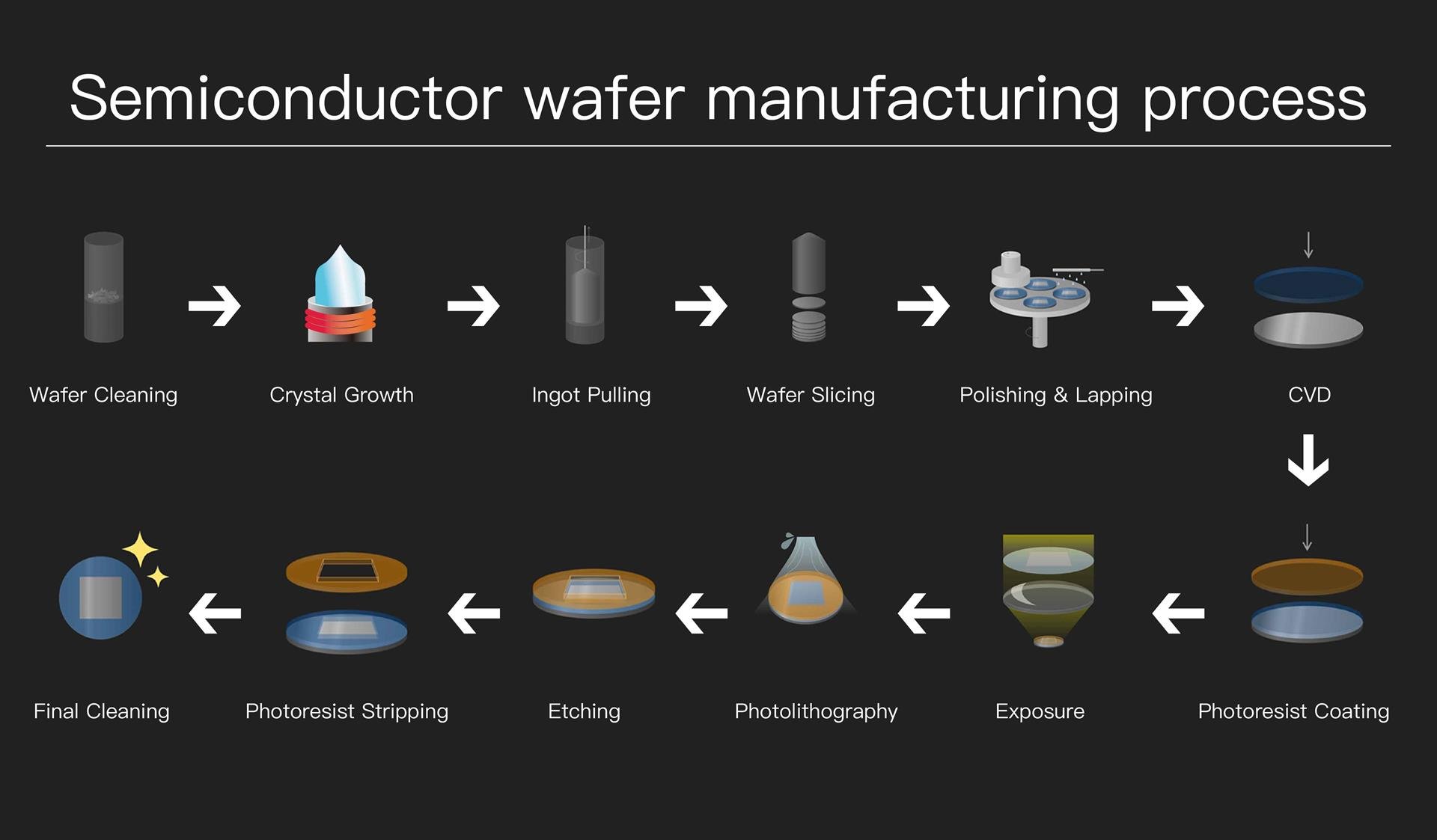
What's the difference between a wafer and a chip? A wafer serves as the initial material for manufacturing chips. It is a thin, circular silicon substrate typically made of single-crystal silicon. The wafer manufacturing process involves two main stages: the first stage, which includes wafer cleaning, crystal growth, ingot pulling, wafer slicing, and polishing; and the second stage, known as wafer fabrication, which includes processes such as vapor deposition, photoresist coating, exposure, developing, etching, photoresist stripping and final cleaning.
Wafer Cleaning
The wafer raw materials' surfaces are cleaned through high-temperature melting and solvents like HF hydrofluoric acid or KOH potassium hydroxide to remove contaminants and organic residues, ensuring excellent substrate quality.
Crystal Growth
High-purity silicon raw material, silicon dioxide, is placed into a furnace for refining, reducing it to metallurgical-grade silicon. After distillation purification, it undergoes a slow decomposition process to produce "polycrystalline silicon.
Ingot Pulling
Polycrystalline silicon is melted with boric acid and phosphorus in a quartz crucible, and then, at high temperatures, a single crystal silicon rod (seed crystal) is immersed and pulled up while rotating. The silicon adheres to the seed crystal and solidifies evenly on the rod, forming a columnar single crystal silicon ingot.
Wafer Slicing
The freshly produced crystal column has an uneven surface. It needs industrial-grade diamond tools for processing, removal of tapered ends, diameter adjustment, and cutting into wafer slices using high-hardness saw blades or wire saws.
Polishing & Lapping
After wafer dicing, the surface becomes rough and requires polishing and grinding. Polishing aims to make the crystal surface smoother and shinier, while grinding rounds the wafer's edges into a smooth curve.
CVD (Chemical Vapor Deposition)
CVD is a process where gaseous precursors are introduced into a reaction chamber. When these gases come into contact with a heated substrate, they generate deposited materials, forming a thin film on the substrate's surface, used for creating insulating or conducting layers.
Photoresist Coating
When exposed, photoresist undergoes a chemical change. Initially, a uniform photoresist layer is coated onto the wafer's surface, allowing it to be removed or retained in subsequent exposure and development steps, forming the desired pattern.
Exposure
Using patterns on the photomask, expose the photoresist layer to ultraviolet light. Align the photomask onto the wafer coated with photoresist, causing a chemical reaction in the photoresist layer in the illuminated areas, initiating a photochemical reaction.
Photolithography
Exposing wafers to a developing solution (possibly containing alkalis like sodium hydroxide, potassium hydroxide, and additives) selectively removes unexposed areas of the photoresist layer, leaving behind a template in the exposed regions.
Etching
Using acidic or alkaline etching solutions, remove underlying materials based on the pattern on the photoresist layer, leaving the protected areas on the wafer surface (exposed photoresist areas) unaffected, shaping the microstructures of the chip.
Photoresist Stripping
After development, residual photoresist is removed through chemical, thermal, or mechanical methods, like stripping solution, to prevent adverse effects on device performance.
Final Cleaning
Finally, the chips undergo a secondary cleaning process, which may involve organic or inorganic solvents, surfactants, or ultrasonic cleaning techniques, to remove residual chemicals and particles from the manufacturing process, ensuring the produced chips are clean and meet specifications.