A Printed Circuit Board (PCB) is an essential component in modern electronics, connecting electronic components on a non-conductive substrate. It's used in a wide range of electronic products, from smartphones to home appliances to industrial automation systems. The complexity of electronic devices necessitates the coordination of numerous components, with the PCB serving as their assembly platform. Essentially, a PCB is a thin board embedded with electronic components and circuits, often including Integrated Circuits (ICs), which are typically soldered onto the PCB. The conductive layers on the PCB facilitate the transmission of electricity and signals among different components, enabling the creation of a functional electronic system to fulfill specific product functions
[1][2]
The integration of Artificial Intelligence into PCB layout design is seen as a transformative step, significantly enhancing the efficiency and optimization of electronic systems engineering. This integration facilitates a new era of design optimization and automation while accelerating product development cycles.
In traditional PCB design, tasks like creating schematics, placing components, routing traces, and optimizing layout for signal integrity and manufacturability were done manually, demanding a deep understanding of electronics and engineering principles. However, the increasing complexity of electronic devices and the demand for higher performance have driven the need for a more intelligent approach to PCB layout. AI, particularly in the form of machine learning and deep learning technologies, is being integrated into Electronic Design Automation tools, revolutionizing PCB design with automated component placement, routing optimization, design rule checking, and other AI-driven enhancements.
The use of AI in PCB layout presents new opportunities for design optimization, but it also brings unique challenges and ethical considerations. AI implementation in PCB design may involve intricate design constraints, interdisciplinary collaboration, regulatory compliance, and data privacy and security concerns. Despite these challenges, AI's role in PCB layout is expected to become even more integral in shaping the future of electronics design.
[4]
Printed Circuit Boards (PCBs) are populated with numerous electronic components and use conductive materials, typically copper traces, as the communication bridge between these components. Depending on product characteristics and applications, PCBs are categorized into various types:
Single-Layer PCB - This type of PCB has a single conductive layer on one side of the board, with the other side used for integrating various electronic circuits. Common in simpler electronic products like calculators and radios, single-layer PCBs are relatively cost-effective.
Double-Layer PCB - In double-layer PCBs, conductive layers are present on both sides of the substrate, separated by an insulating layer. Components on both sides are connected through plated-through holes, allowing for more compact circuit designs. This type is suitable for moderately complex electronics such as digital cameras, measuring instruments, and gaming controllers.
Multi-Layer PCB - These PCBs contain multiple layers of copper foil separated by insulating material, all bonded together under high pressure and temperature for durability. Multi-layer PCBs enable high integration and complex circuit designs, making them ideal for advanced electronic products like data storage devices, satellite systems, medical equipment, and GPS devices.
Rigid PCB - Also known as hard PCB, this type typically utilizes glass fiber-reinforced epoxy resin (FR-4) as the base material. Rigid PCBs are sturdy and non-flexible, commonly used in central processing units (CPUs) of computer motherboards, medical monitoring devices, and industrial automation equipment.
Rigid-Flex PCBs – Also known as Rigid-Flexible Printed Circuit Boards or Rigid-Flex boards, these combine rigid and flexible areas, interconnected through Flex Connectors. Precision alignment and lamination are essential for bonding, while multilayer interconnections are achieved using Plated Through Holes (PTH). Rigid-flex PCBs are utilized in foldable devices and embedded medical equipment.
Flexible PCBs – Commonly referred to as Flex PCBs, these are made using flexible substrate materials like Polyester or Polyimide films. Characterized by their bendability and lightweight nature, they have higher production costs and are ideal for space-constrained applications requiring flexibility, such as in displays, smartwatches, aerospace instrument panels, and entertainment systems.
High-Frequency PCBs – Designed for high-frequency signals and microwave applications, these PCBs require Impedance Control to avoid signal reflection due to Electromagnetic Interference (EMI) and Radio Frequency Interference (RFI). High-frequency PCBs demand advanced technical expertise in design and manufacturing, often used in wireless communication devices and radar systems.
HDI PCBs (High-Density Interconnect PCB) – These utilize Microvias, Blind Vias, and Buried Vias along with BGA packaging to achieve high integration and dense connections. HDI PCBs are typically employed in high-performance electronics like smartphones, tablets, and sophisticated communication devices, catering to demands for miniaturization, lightweight, and enhanced performance.
Metal Core PCBs – Utilizing metal as the base material instead of traditional Fiberglass, Metal Core PCBs offer superior heat dissipation. They are commonly used in high-heat applications such as LED lighting and solar converters.
[5][6][7]

STEP 1: Sheets Cutting
Cut the substrate into the required dimensions.
STEP 2: Dry Film Lamination
Cover the surface of the board with a photosensitive organic film, and after exposure, transfer the circuit pattern from the film to the board.
STEP 3: Exposure
Insert the board with the dry film attached into the exposure machine for exposure. The dry film undergoes photosensitive hardening after being exposed to UV light in the transparent area of the film. This process transfers the circuit image from the film onto the surface of the board.
STEP 4: Inner Developing
Dissolve the non-photosensitive dry film in the developer solution to create the inner layer circuit pattern.
STEP 5: Inner Etching
After the undeveloped dry film dissolves, the underlying copper surface becomes exposed. The board then undergoes an etching process, where the exposed copper surface is dissolved by the etching solution, revealing the substrate beneath. The copper surface adhered with the dry film remains intact, forming the inner circuitry.
STEP 6: Inner Stripping
Use a film removal solution to remove the photohardened dry film.
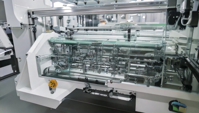
STEP 7: Drilling
In the PCB drilling process, several types of holes are formed, including via holes (like thru-holes, buried holes, blind holes, and micro-holes), along with component and mechanical holes. Due to the need for accuracy, these holes are generally produced using either a manual drill or a laser PCB drill. We manufacture various components such as holes for customer requirements, mounting holes, through holes, and provide positioning holes required for post-processing. We also provide inspection slots when quality control is needed.
STEP 8: PTH Plating
The process of through-hole electroplating, also known as one-shot copper plating, involves chemically depositing a thin layer of copper inside non-conductive resin or glass fiber holes. This process aims to metallize the hole walls and enable the connection between inner and outer circuit layers.
STEP 9: Developing
Disolve the unexposed dry film on the outer layer of the circuit board.
STEP 10: Pattern Plating, Tin-Lead Plating
After development, the next step involves double copper and tin-lead plating, aiming to increase the thickness of the outer layer of the circuit. The purpose of tin plating is to protect the copper beneath it from being dissolved by the etching solution in the subsequent process.
STEP 11: Stripping, Etching, Tin-Lead Stripping
Using a de-coating solution, the dry film on the board's surface is removed, exposing the copper layer underneath. After etching with an etching solution, the exposed copper layer is dissolved, revealing the substrate. The copper surface coated with tin remains unaffected due to the tin's protective layer, forming the outer circuitry. Finally, all the tin-lead on the board's surface is removed using a tin-lead stripping solution.
STEP 12: Solder Mask
After preprocessing, the board is cleaned, and a layer of solder-resistant photosensitive ink is applied to the surface. After a preliminary drying process, it undergoes an exposure operation. Following exposure, the unsensitized solder-resistant ink dissolves in the developer solution, while the photosensitive solder-resistant ink, once hardened by exposure, remains unaffected and forms the solder mask pattern on the board surface.
STEP 13: Surface Treatment
The purpose is to prevent surface oxidation.
STEP 14: Profiling
Perform external processing and cutting to create sizes that meet customer requirements.
STEP 15: Electrical Testing
Conduct a check on the circuitry of the board and test the electrical functionality of the board.
STEP 16: Final Visual Inspection
Inspect the product's appearance comprehensively to ensure the quality of the shipped goods.
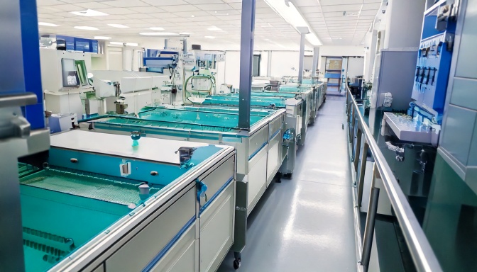
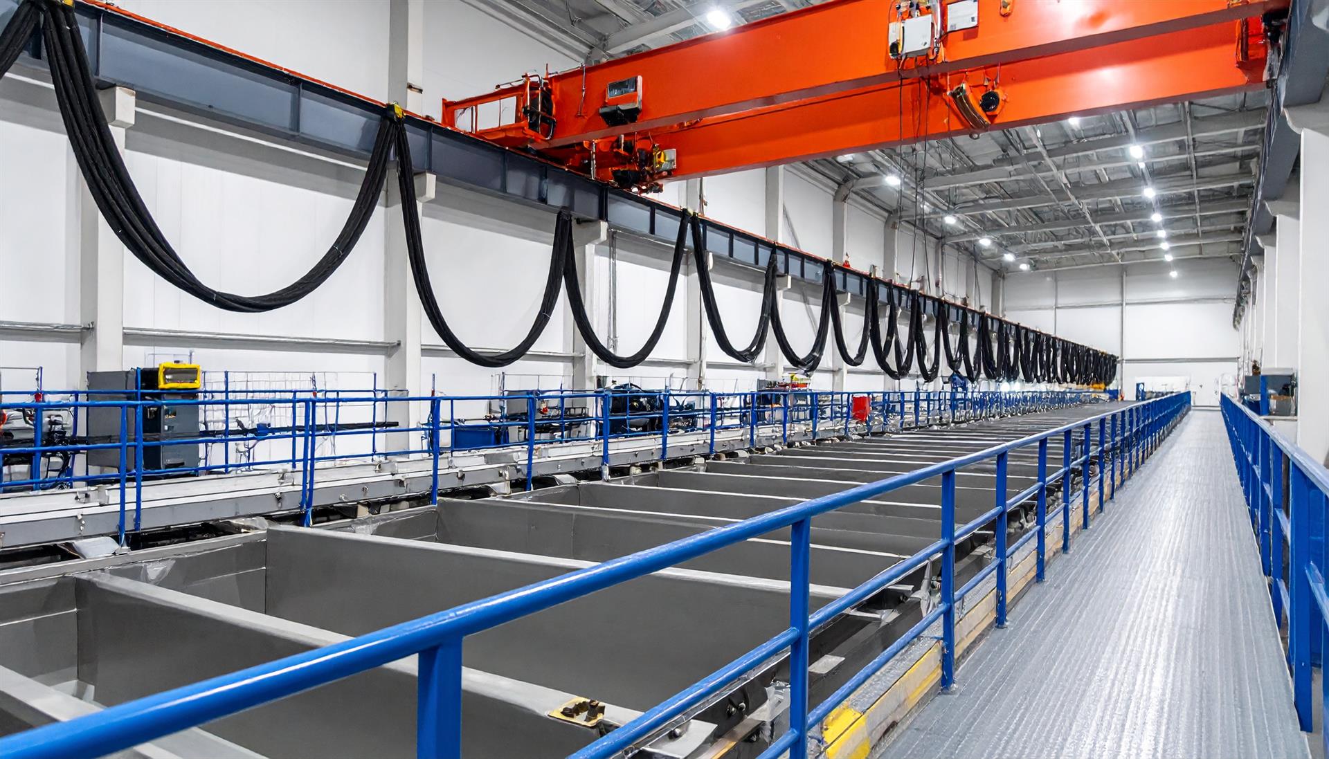
The process of manufacturing printed circuit boards involves numerous steps such as electroplating, development, etching, and cleaning, requiring a variety of chemical agents for processing. Within these processes, factors like the quantity and distribution of sprayed chemicals, the contact time between liquids and materials, and even the force with which chemicals impact the board can all impact the quality of the final product; that is why having high-quality nozzles is crucial. Additionally, by using liquid flow meters to measure the dosage of chemical agents, manufacturers can more precisely regulate material flow, leading to higher-quality products and increased production efficiency.
Application 1: Spray of Liquid for Plating Residue Removal in Through-Hole Electroplating
Case: Global Renowned Electronic Equipment Integration Manufacturer
Situation: The company has developed horizontal chemical copper equipment (DSM & PTH) that effectively removes residue glue from circuit board holes after the through-hole electroplating process, ensuring optimal conductivity performance in subsequent production steps. Removing this residue requires the use of various chemical agents, prompting the company to seek corrosion-resistant and effective nozzles.
Solution: LORRIC's QF Series Quick-Disconnect Nozzles
The QF Series Quick-Disconnect Nozzles, manufactured from high-quality engineering plastics (PP, PVDF), offer exceptional chemical resistance, prolonging the nozzle's lifespan. Furthermore, the QF Series nozzles feature a multi-part quick-disconnect design. Once installed, if nozzle replacement is required, simply detach the nozzle head from the base and replace it, eliminating the need for repositioning the nozzle, streamlining machine maintenance and servicing. In addition to nozzle products, we recommend using LORRIC's area flow meters to measure the quantity of chemicals used in the electroplating process. LORRIC's area flow meters are precision-engineered and rigorously tested in our flow measurement laboratory, with errors controlled within the industry's top ±5% F.S. standard. The flow meter body and fittings are made of high-quality plastics, providing excellent corrosion resistance and effectively extending the product's lifespan.
Application 2: Monitoring Copper Sulfate Solution in Electroplating Process
Case: Top 10 PCB Manufacturer in South Korea
Situation: Established in 1987, this company specializes in developing module PCBs for DRAM memory chips and substrates for various semiconductor chip assembly processes. As of 2022, it ranks among South Korea's top 10 printed circuit board suppliers. Initially, the company used paddlewheel flow meters from a German brand in its electroplating process line to measure the usage of copper sulfate solution. Due to safety regulations in South Korea, all equipment using chemicals is required to be separated from the work environment using transparent partitions. However, this setup made it difficult for workers to read flow data on traditional LCD screens through the partitions.
Solution: LORRIC's FP-AS510 Paddlewheel Flow Meter
The FP-AS510 Paddlewheel Flow Meter features a dual LED/LCD screen design and includes contextual indicators, allowing workers to easily read flow rates and monitor machine status even in low-light working conditions or through partitioned areas. Additionally, the FP-AS510 utilizes patented shaft sensing technology, enabling flow detection at extremely low speeds (0.15 m/s) with an industry-leading linearity of 0.5% FS. It also offers three communication options (4-20mA analog output, Modbus RTU RS485 control signal, and optical coupler pulse signal) to meet diverse customer communication requirements seamlessly.
Application 3: Monitoring of Strong Acid and Alkali Solutions in Vertical Continuous Plating Equipment
Case: Top Five PCB Manufacturers Worldwide
Situation: The company employs Vertical Continuous Plating Line to significantly improve the distribution efficiency of electroplating and maintain consistent plating quality for each panel. The Vertical Continuous Plating Line utilizes various chemical agents, and LORRIC's area-based flow meters, made of high-quality plastics with strong chemical resistance, effectively reduce equipment maintenance frequency and costs in the face of strong acid and alkali solutions.
Solution: FU-ES EchoSense Clamp-On Ultrasonic Flow Meter
As precision requirements for printed circuit boards continue to rise, many manufacturers prefer ultrasonic flow meters that do not come into direct contact with chemical solutions. Addressing this demand, LORRIC has developed the new FU-ES EchoSense Clamp-On Ultrasonic Flow Meter. This product is specifically designed for small-diameter applications. Its integrated design combines the probe and the main unit, allowing for a quick 90-second installation. Furthermore, the device can automatically detect pipe specifications (material, thickness, liquid sound speed, etc.), making machine setup as simple as a button press. The part of the probe in contact with the pipe is now equipped with rubber coupling pads, eliminating the need for ultrasound gel and simplifying device maintenance.